NEET Ug . NEET Physics . Physics . Semiconductor Electronics Materials Devices and Simple Circuits
Chapter 29: Semiconductor Electronics: Materials, Devices and Simple Circuits
Ch 29
NEET Physics
NEET Ug
Introduction
Overview of Electronic Devices
- Early electronic devices: vacuum tubes (diode, triode, tetrode, pentode).
- Vacuum tubes: bulky, high power consumption, high voltage (~100 V), limited life, low reliability.
- Modern electronics use solid-state semiconductors for controlled electron flow.
- Semiconductors' charge carriers can be controlled by light, heat, or voltage.
- CRT displays replaced by LCD monitors due to semiconductor technology.
Solved Examples
Ex 1
Identify the main disadvantage of vacuum tubes compared to semiconductors.
- Answer: High power consumption and bulkiness.
Practice Set
- Q1: Which device is bulky and consumes high power?
A) Transistor
B) Vacuum tube
C) Diode
D) LED - Q2: What replaces CRT monitors in modern electronics?
A) Vacuum tubes
B) LCD monitors
C) Cathode ray tubes
D) Pentodes - Q3: Which excitation can change mobile charge carriers in semiconductors?
A) Light
B) Heat
C) Small voltage
D) All of the above
Answer Key
- Q1: B - Vacuum tubes are bulky and consume high power.
- Q2: B - LCD monitors replaced CRTs due to semiconductor tech.
- Q3: D - Light, heat, and voltage affect charge carriers in semiconductors.
Memory Aids
- Vacuum tubes = bulky + high power.
- Semiconductors = controlled electron flow.
- LCD replaces CRT in displays.
Classification of Metals, Conductors and Semiconductors
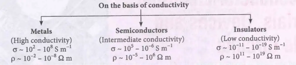
Material Classification by Conductivity
- Conductivity (σ) measures ease of electric current flow.
- Metals: high conductivity, electricity flows easily.
- Semiconductors: medium conductivity, moderate current flow.
- Insulators: very low conductivity, negligible current flow.
- Conductivity and resistivity (ρ) are inversely related: \( \sigma = \frac{1}{\rho} \).
Solved Examples
Ex 1
Classify a material with conductivity \(10^7\) S/m.
- Answer: Metal (high conductivity).
Practice Set
- Q1: Which has the highest conductivity?
A) Metal
B) Semiconductor
C) Insulator
D) Vacuum - Q2: Resistivity and conductivity are:
A) Directly proportional
B) Inversely proportional
C) Equal
D) Unrelated - Q3: Which material allows moderate current flow?
A) Metal
B) Semiconductor
C) Insulator
D) Vacuum tube
Answer Key
- Q1: A - Metals have highest conductivity.
- Q2: B - Resistivity and conductivity are inversely proportional.
- Q3: B - Semiconductors allow moderate current flow.
Memory Aids
- Metal = High σ, low ρ.
- Semiconductor = Medium σ.
- Insulator = Low σ, high ρ.
Energy Bands of Solids or Band Theory of Solids
Key Energy Bands
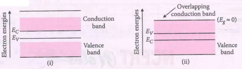
- Valence band: Contains valence electrons; fully or partially filled; electrons do not conduct current.
- Conduction band: Empty or partially filled; contains free electrons that conduct current.
- Forbidden energy gap (band gap): Energy gap between valence and conduction bands; no electrons present here.
- Energy band gap formula: \( E_g = h \nu = \frac{hc}{\lambda} \), where \(h\) = Planck's constant, \(c\) = speed of light, \(\lambda\) = wavelength.
- Band gap varies with temperature.
- Fermi energy: Maximum energy of free electrons at 0 K.
Solved Examples
Ex 1
Calculate band gap if wavelength \(\lambda = 620\) nm. Use \(h = 6.63 \times 10^{-34}\) Js, \(c = 3 \times 10^8\) m/s, \(1 eV = 1.6 \times 10^{-19}\) J.
- \(E_g = \frac{hc}{\lambda} = \frac{6.63 \times 10^{-34} \times 3 \times 10^8}{620 \times 10^{-9}} = 3.21 \times 10^{-19}\) J
- Convert to eV: \(\frac{3.21 \times 10^{-19}}{1.6 \times 10^{-19}} = 2.0\) eV
Practice Set
- Q1: Electrons in which band conduct electricity?
A) Valence band
B) Conduction band
C) Forbidden gap
D) Fermi level - Q2: Band gap \(E_g\) is energy difference between:
A) Valence and conduction bands
B) Two valence bands
C) Two conduction bands
D) Electron and hole - Q3: If \(\lambda = 500\) nm, calculate \(E_g\) in eV. (Use \(h=6.63\times10^{-34}\) Js, \(c=3\times10^8\) m/s, \(1 eV=1.6\times10^{-19}\) J)
A) 2.48 eV
B) 1.24 eV
C) 3.10 eV
D) 4.00 eV
Answer Key
- Q1: B - Conduction band electrons conduct current.
- Q2: A - Band gap is between valence and conduction bands.
- Q3: A - \(E_g = \frac{6.63\times10^{-34} \times 3\times10^8}{500\times10^{-9}} = 3.98\times10^{-19} J = 2.48 eV\).
Memory Aids
- Band gap formula: \(E_g = \frac{hc}{\lambda}\).
- Conduction band = free electrons.
- Valence band = bound electrons.
Energy Bands Based on Material Type
Metals
- Conduction band partially filled or overlaps valence band.
- No forbidden energy gap.
- Electrons move freely, high conductivity.
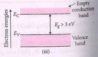
Insulators
- Valence band fully filled; conduction band empty.
- Large forbidden energy gap (>5 eV).
- Very low conductivity.
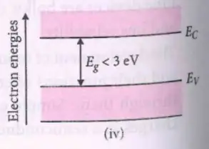
Semiconductors
- Valence band fully filled; conduction band empty at 0 K.
- Small forbidden energy gap (~1 eV): Silicon (1.1 eV), Germanium (0.72 eV).
- Conductivity increases with temperature.
Solved Examples
Ex 1
Identify the material type with band gap 0.7 eV.
- Answer: Semiconductor (e.g., Germanium).
Practice Set
- Q1: Which material has no band gap?
A) Metal
B) Semiconductor
C) Insulator
D) Vacuum tube - Q2: Band gap of silicon is approximately:
A) 0.5 eV
B) 1.1 eV
C) 3 eV
D) 5 eV - Q3: Which material has a band gap > 5 eV?
A) Metal
B) Semiconductor
C) Insulator
D) None
Answer Key
- Q1: A - Metals have no band gap.
- Q2: B - Silicon band gap is ~1.1 eV.
- Q3: C - Insulators have band gap > 5 eV.
Memory Aids
- Metal: No band gap.
- Semiconductor: Small band gap (~1 eV).
- Insulator: Large band gap (>5 eV).
Hole in Semiconductors
Definition and Properties
- Hole: Positive charge carrier formed when electron leaves covalent bond.
- Charge of hole = +e (same magnitude as electron charge).
- Hole mobility is less than electron mobility.
Solved Examples
Ex 1
What charge does a hole carry?
- Answer: Positive charge equal to electron charge.
Practice Set
- Q1: A hole is:
A) Negative charge carrier
B) Positive charge carrier
C) Neutral particle
D) Electron - Q2: Hole mobility compared to electron mobility is:
A) Greater
B) Equal
C) Smaller
D) Zero - Q3: Hole is created when:
A) Electron breaks covalent bond
B) Electron recombines
C) Electron moves to valence band
D) Electron is created
Answer Key
- Q1: B - Hole carries positive charge.
- Q2: C - Hole mobility is smaller than electron mobility.
- Q3: A - Hole forms when electron breaks covalent bond.
Memory Aids
- Hole = positive charge carrier.
- Mobility: electron > hole.
- Hole forms by electron leaving bond.
Intrinsic Semiconductor
Definition and Examples
- Pure semiconductor without impurities is called intrinsic semiconductor.
- Examples: Silicon (Si), Germanium (Ge).
Carrier Concentrations
- Number density of electrons in conduction band, \( n_e \).
- Number density of holes in valence band, \( n_h \).
- Intrinsic carrier concentration, \( n_i \).
- In intrinsic semiconductor, \( n_e = n_h = n_i \).
Current and Conductivity
- Total current, \( I = I_e + I_h \), where \( I_e \) is electron current and \( I_h \) is hole current.
- Conductivity, \( \sigma = n_i e (\mu_e + \mu_h) \), where \( e \) is electron charge, \( \mu_e \) and \( \mu_h \) are mobilities.
- Resistivity, \( \rho = \frac{1}{\sigma} = \frac{1}{e n_i (\mu_e + \mu_h)} \).
- Current, \( I = n_i e A (v_e + v_h) \), where \( A \) is cross-sectional area, \( v_e \) and \( v_h \) are drift velocities.
Temperature Effect
- Increasing temperature increases electron-hole pair density \( \Rightarrow \) conductivity increases.
- Resistivity decreases with temperature.
- Semiconductors have negative temperature coefficient of resistance.
Crystal Structure and Hole Motion
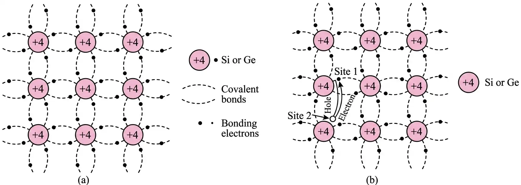
- Si or Ge atoms form covalent bonds with four neighbors (+4 core charge).
- At low temperature, all bonds intact.
- Electron movement from one bond to hole site causes apparent hole motion.
- Hole acts as positive charge carrier moving through lattice.
Solved Examples
Ex 1
Calculate conductivity if \( n_i = 1.5 \times 10^{16} \text{ m}^{-3} \), \( \mu_e = 0.14 \text{ m}^2/\text{V·s} \), \( \mu_h = 0.05 \text{ m}^2/\text{V·s} \), and \( e = 1.6 \times 10^{-19} \text{ C} \).
- Use \( \sigma = n_i e (\mu_e + \mu_h) \).
- \( \sigma = 1.5 \times 10^{16} \times 1.6 \times 10^{-19} \times (0.14 + 0.05) = 3.456 \times 10^{-3} \text{ S/m} \).
Practice Set
Q1
In an intrinsic semiconductor, the number density of electrons is:
- A) Greater than holes
- B) Less than holes
- C) Equal to holes
- D) Zero
Q2
Which of the following increases conductivity of intrinsic semiconductor?
- A) Decreasing temperature
- B) Increasing temperature
- C) Adding impurities
- D) Decreasing carrier mobility
Q3
Calculate resistivity if \( n_i = 2 \times 10^{16} \text{ m}^{-3} \), \( \mu_e = 0.15 \text{ m}^2/\text{V·s} \), \( \mu_h = 0.05 \text{ m}^2/\text{V·s} \), and \( e = 1.6 \times 10^{-19} \text{ C} \).
- A) \( 1.56 \times 10^{2} \, \Omega\cdot m \)
- B) \( 3.12 \times 10^{2} \, \Omega\cdot m \)
- C) \( 1.56 \times 10^{-2} \, \Omega\cdot m \)
- D) \( 3.12 \times 10^{-2} \, \Omega\cdot m \)
Answer Key
- Q1: C) Equal to holes — Intrinsic semiconductors have equal electron and hole densities.
- Q2: B) Increasing temperature — Higher temperature generates more electron-hole pairs, increasing conductivity.
- Q3: A) \( 1.56 \times 10^{2} \, \Omega\cdot m \) — \( \rho = \frac{1}{e n_i (\mu_e + \mu_h)} = \frac{1}{1.6 \times 10^{-19} \times 2 \times 10^{16} \times 0.2} = 156 \ \Omega\cdot m \).
Memory Aids
- Intrinsic: \( n_e = n_h = n_i \).
- Conductivity \( \sigma = n_i e (\mu_e + \mu_h) \).
- Resistivity \( \rho = 1/\sigma \).
- Conductivity ↑ with temperature ↑ (negative TCR).
- Hole motion = electron hopping in covalent bonds.
Energy Band Diagram
Band Structure at Different Temperatures
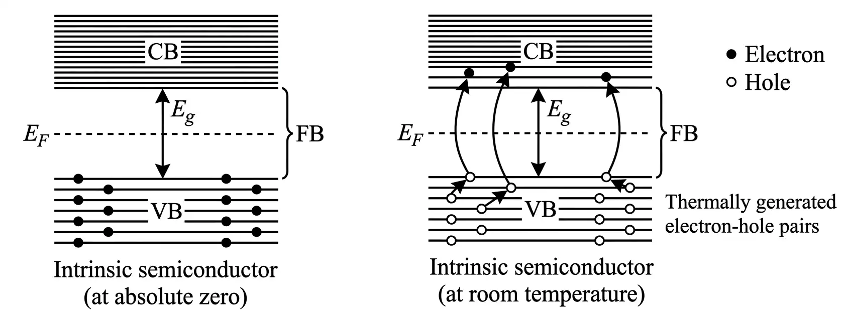
- At \( T=0 \text{ K} \), valence band (VB) fully filled, conduction band (CB) empty.
- Intrinsic semiconductor behaves as insulator at 0 K.
- At \( T>0 \text{ K} \), electrons gain thermal energy and jump from VB to CB.
- Equal number of holes created in VB.
- Electrons occupy lowest energy states in CB.
- Number of electrons in CB equals number of holes in VB.
Solved Examples
Ex 1
Explain conduction at 0 K and room temperature.
- At 0 K: No electrons in CB, no conduction.
- At room temperature: Thermal excitation creates electron-hole pairs, enabling conduction.
Practice Set
Q1
At absolute zero, an intrinsic semiconductor is:
- A) Conductor
- B) Insulator
- C) Semiconductor
- D) Superconductor
Q2
Electron-hole pairs in intrinsic semiconductor are created by:
- A) Impurities
- B) Thermal energy
- C) Electric field only
- D) Magnetic field
Q3
At room temperature, the number of electrons in conduction band is:
- A) Less than holes in valence band
- B) Equal to holes in valence band
- C) Greater than holes in valence band
- D) Zero
Answer Key
- Q1: B) Insulator — At 0 K, no free carriers, so no conduction.
- Q2: B) Thermal energy — Heat excites electrons to conduction band.
- Q3: B) Equal to holes in valence band — Electron-hole pairs are created in equal numbers.
Memory Aids
- 0 K: VB full, CB empty, no conduction.
- \( T>0 \): Thermal excitation creates equal electron-hole pairs.
- Electron-hole pairs enable conduction.
Extrinsic Semiconductor
Concepts
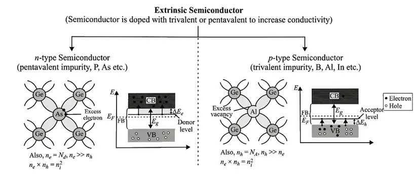
- Impure semiconductor with added impurities is called extrinsic semiconductor.
- Doping: Adding small amounts of impurities with different valency to pure semiconductor.
- Doping changes number of mobile charge carriers (electrons or holes), increasing conductivity.
- Two types: n-type (pentavalent impurities) and p-type (trivalent impurities).
- Energy band diagrams show donor and acceptor levels affecting electron movement.
Solved Examples
Ex 1: Identify majority carriers in n-type semiconductor doped with phosphorus.
- Phosphorus is pentavalent impurity (group V).
- Donates extra electrons.
- Majority carriers are electrons (negative charge).
Practice Set
- Q1: What is doping in semiconductors?
A) Removing impurities
B) Adding impurities to increase conductivity
C) Heating semiconductor
D) Cooling semiconductor - Q2: In n-type semiconductor, majority carriers are:
A) Holes
B) Electrons
C) Ions
D) Neutrons - Q3: Which impurity is used for p-type doping?
A) Phosphorus
B) Arsenic
C) Boron
D) Antimony
Answer Key
- Q1: B - Doping means adding impurities to increase conductivity.
- Q2: B - Electrons are majority carriers in n-type semiconductor.
- Q3: C - Boron (trivalent) is used for p-type doping.
Memory Aids
- Doping = Adding impurities to increase conductivity.
- n-type: Donor atoms (group V), electrons majority.
- p-type: Acceptor atoms (group III), holes majority.
n-type Semiconductor
Concepts
- Pure Si or Ge (tetravalent) doped with pentavalent impurities (As, Sb, P).
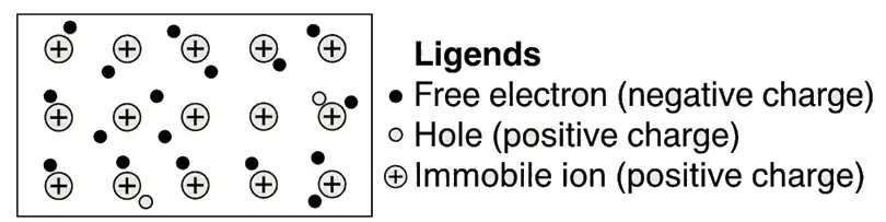
- Donor atoms donate one free electron each for conduction.
- Conduction due to electrons (negative charge carriers).
- Electrons are majority carriers; holes are minority carriers.
- Charge neutrality maintained.
- Carrier concentration: \( n_e \approx N_d \gg n_h \), where \( N_d \) = donor density.
Solved Examples
Ex 1: Calculate majority carrier concentration if donor density \( N_d = 10^{16} \) cm-3.
- Majority carrier concentration \( n_e \approx N_d = 10^{16} \) cm-3.
Practice Set
- Q1: Donor atoms in n-type semiconductor are from group:
A) III
B) IV
C) V
D) VI - Q2: Majority carriers in n-type semiconductor are:
A) Holes
B) Electrons
C) Ions
D) Protons - Q3: If donor density is \( 5 \times 10^{15} \) cm-3, approximate electron concentration is:
A) \( 5 \times 10^{15} \) cm-3
B) \( 5 \times 10^{14} \) cm-3
C) \( 10^{16} \) cm-3
D) \( 10^{14} \) cm-3
Answer Key
- Q1: C - Donor atoms are pentavalent (group V).
- Q2: B - Electrons are majority carriers in n-type.
- Q3: A - Electron concentration \( \approx N_d = 5 \times 10^{15} \) cm-3.
Memory Aids
- n-type = Negative charge carriers (electrons).
- Donor atoms = group V elements.
- Majority carriers \( n_e \approx N_d \).
p-type Semiconductor
Concepts
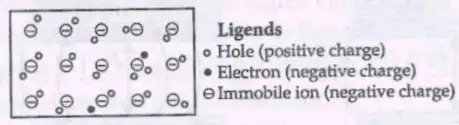
- Pure Si or Ge doped with trivalent impurities (Al, B, In).
- Acceptor atoms create holes by accepting electrons.
- Conduction due to holes (positive charge carriers).
- Holes are majority carriers; electrons are minority carriers.
- Charge neutrality maintained.
- Carrier concentration: \( n_h \approx N_a \gg n_e \), where \( N_a \) = acceptor density.
Solved Examples
Ex 1: Find majority carrier concentration if acceptor density \( N_a = 2 \times 10^{16} \) cm-3.
- Majority carrier concentration \( n_h \approx N_a = 2 \times 10^{16} \) cm-3.
Practice Set
- Q1: Acceptor atoms in p-type semiconductor belong to group:
A) III
B) IV
C) V
D) VI - Q2: Majority carriers in p-type semiconductor are:
A) Electrons
B) Holes
C) Ions
D) Neutrons - Q3: If acceptor density is \( 1 \times 10^{15} \) cm-3, hole concentration is approximately:
A) \( 1 \times 10^{15} \) cm-3
B) \( 1 \times 10^{14} \) cm-3
C) \( 10^{16} \) cm-3
D) \( 10^{14} \) cm-3
Answer Key
- Q1: A - Acceptor atoms are trivalent (group III).
- Q2: B - Holes are majority carriers in p-type.
- Q3: A - Hole concentration \( \approx N_a = 1 \times 10^{15} \) cm-3.
Memory Aids
- p-type = Positive charge carriers (holes).
- Acceptor atoms = group III elements.
- Majority carriers \( n_h \approx N_a \).
p-n Junction
Formation and Charge Distribution
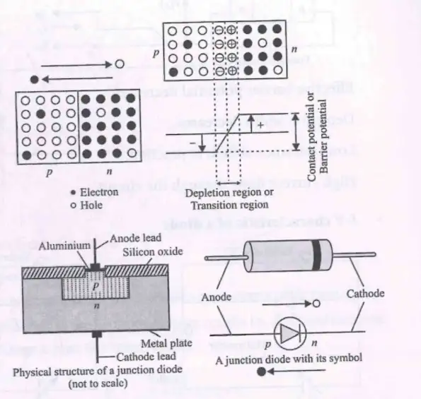
- p-n junction formed by joining p-type (holes) and n-type (electrons) semiconductors.
- Electrons diffuse from n-side to p-side, filling holes; holes diffuse from p-side to n-side.
- Creates positive charge layer on n-side and negative charge layer on p-side near junction.
- These immobile charges form the depletion layer, preventing further charge carrier movement.
- Potential barrier (V₀) of 0.1–0.3 V (0.3 V for Ge, 0.7 V for Si) develops across junction.
- Electric field intensity across depletion region: E = V/d, where V = potential barrier, d = depletion width.
Current Types in p-n Junction
- Diffusion current: Due to concentration gradient, holes move p → n and electrons n → p.
- Drift current: Minority carriers move across junction due to barrier potential.
Solved Examples
- Ex 1: Calculate electric field intensity if potential barrier V = 0.7 V and depletion width d = 2 \(\mu\)m.
- Use E = V/d
- E = 0.7 V / 2 × 10⁻⁶ m = 3.5 × 10⁵ V/m
Practice Set
- Q1: What is the typical potential barrier for silicon p-n junction?
- A) 0.1 V
- B) 0.3 V
- C) 0.7 V
- D) 1.0 V
- Q2: Which current is caused by minority carriers moving due to barrier potential?
- A) Diffusion current
- B) Drift current
- C) Conduction current
- D) Displacement current
- Q3: If the depletion width is 1 \(\mu\)m and potential barrier is 0.3 V, what is the electric field intensity?
- A) 3 × 10⁵ V/m
- B) 3 × 10⁴ V/m
- C) 3 × 10⁶ V/m
- D) 3 × 10³ V/m
Answer Key
- Q1: C) 0.7 V — Silicon p-n junction has a potential barrier around 0.7 V.
- Q2: B) Drift current — Minority carriers move due to barrier potential causing drift current.
- Q3: A) 3 × 10⁵ V/m — E = V/d = 0.3 V / 1 × 10⁻⁶ m = 3 × 10⁵ V/m.
Memory Aids
- Potential barrier: Si ~0.7 V, Ge ~0.3 V.
- Depletion layer = immobile charges, no free carriers.
- Diffusion current: majority carriers move due to concentration gradient.
- Drift current: minority carriers move due to electric field.
- Electric field intensity formula: E = V/d.
Semiconductor Diode
Basic Structure and Function
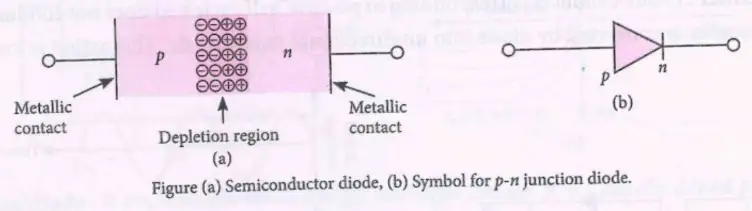
- Formed by joining p-type and n-type semiconductors creating a p-n junction.
- Metallic contacts are attached at ends for external voltage application.
- Depletion region forms at junction, acting as a barrier to current.
- Allows current flow mainly in one direction (p-side to n-side) under forward bias.
- Symbol: Arrow indicates conventional current direction in forward bias.
Solved Examples
- Ex 1: Identify the direction of current flow in a forward biased diode.
- Current flows from p-side to n-side (arrow direction).
Practice Set
- Q1: What forms the depletion region in a semiconductor diode?
- A) Metallic contacts
- B) Junction of p-type and n-type materials
- C) External battery
- D) Insulating layer
- Q2: The arrow in the diode symbol indicates:
- A) Electron flow direction
- B) Conventional current direction under forward bias
- C) Direction of applied voltage
- D) Direction of reverse bias
- Q3: What happens to current flow when a diode is forward biased?
- A) Current flows easily from p to n side
- B) Current is blocked
- C) Current flows from n to p side
- D) No current flows
Answer Key
- Q1: B - Depletion region forms at the junction of p-type and n-type materials.
- Q2: B - Arrow shows conventional current direction when diode is forward biased.
- Q3: A - Forward bias reduces barrier, allowing current from p to n side.
Memory Aids
- Diode = p-n junction + metal contacts.
- Arrow in symbol = forward current direction.
- Depletion region blocks current unless forward biased.
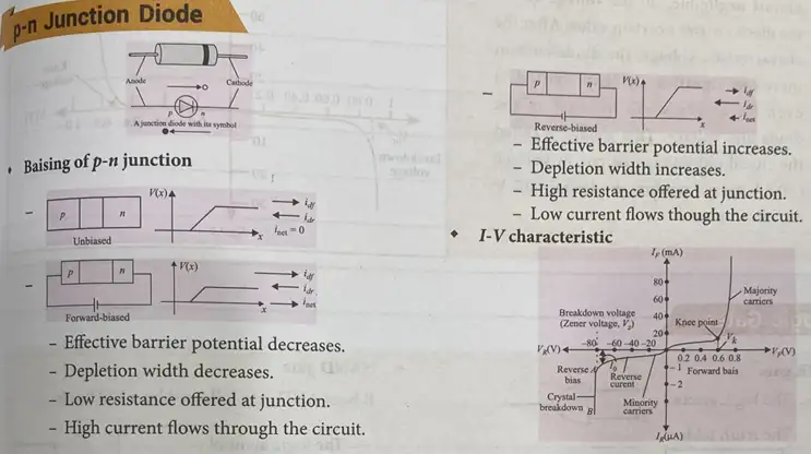
Biasing of p-n Junction
Unbiased Junction
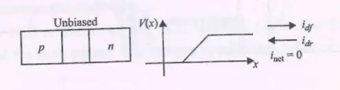
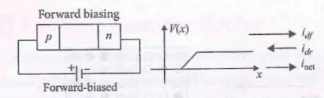
- No external voltage applied.
- Diffusion current (idf) balances drift current (idr).
- Net current (inet) = 0.
- Built-in potential barrier exists across depletion region.
Forward Bias
- Positive terminal connected to p-side, negative to n-side.
- External voltage reduces barrier potential.
- Depletion width decreases.
- Low resistance at junction; high current flows.
- Net current flows in forward direction.
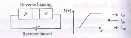
Reverse Bias
- Positive terminal connected to n-side, negative to p-side.
- Barrier potential increases.
- Depletion width increases.
- High resistance at junction; very low leakage current flows.
- Net current is almost zero.
Solved Examples
- Ex 1: What happens to depletion width when a diode is forward biased?
- Depletion width decreases.
- Ex 2: Describe current flow in reverse bias.
- Very small leakage current; net current nearly zero.
Practice Set
- Q1: In forward bias, the barrier potential:
- A) Increases
- B) Decreases
- C) Remains same
- D) Becomes zero
- Q2: Reverse bias causes:
- A) Decrease in depletion width
- B) Increase in depletion width
- C) No change in depletion width
- D) Current flow from p to n side
- Q3: Which of the following is true for reverse biased diode?
- A) High current flows
- B) Low resistance at junction
- C) Net current is almost zero
- D) Barrier potential decreases
Answer Key
- Q1: B - Forward bias reduces barrier potential.
- Q2: B - Reverse bias increases depletion width.
- Q3: C - Net current is nearly zero in reverse bias.
Memory Aids
- Forward bias: Barrier down, width down, current up.
- Reverse bias: Barrier up, width up, current negligible.
- Depletion region controls current flow.
I-V Characteristic of Diode
Key Points
- Current through diode: \( I = I_0 \left[ e^{\frac{eV}{nkT}} - 1 \right] \)
- Where:
- \( I_0 \) = reverse saturation current
- \( e \) = electronic charge
- \( V \) = applied voltage
- \( n \) = ideality factor (1 for Ge, 2 for Si)
- \( k \) = Boltzmann constant
- \( T \) = absolute temperature (K)
- Dynamic resistance: \( r_d = \frac{\Delta V}{\Delta I} \)
- Static (dc) resistance: \( r_{dc} = \frac{V}{I} \)
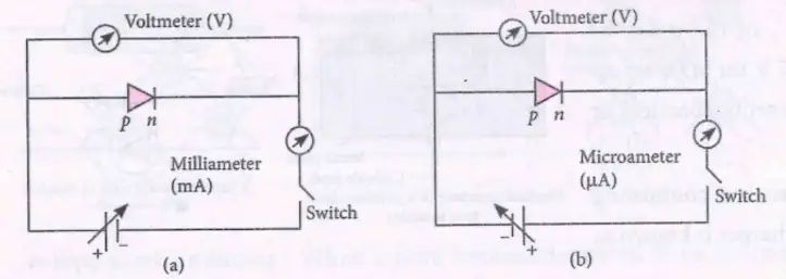
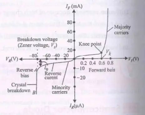
- Forward bias: Current increases exponentially after threshold voltage.
- Reverse bias: Current is very small (reverse saturation current) until breakdown.
Zener Diode Characteristics
- Forward bias similar to normal diode.
- Reverse bias shows breakdown at Zener voltage \( V_Z \).
- At \( V_Z \), current increases sharply without damage.
- Used for voltage regulation.
Solved Examples
- Ex 1: Calculate current if \( V = 0.7V \), \( I_0 = 10^{-12} A \), \( n=1 \), \( T=300K \).
- Use formula \( I = I_0 [e^{eV/nkT} -1] \).
Practice Set
- Q1: In the diode equation, the ideality factor \( n \) is:
- A) 1 for Si, 2 for Ge
- B) 2 for Si, 1 for Ge
- C) Always 1
- D) Always 2
- Q2: Dynamic resistance \( r_d \) is defined as:
- A) \( V/I \)
- B) \( \Delta V / \Delta I \)
- C) \( I/V \)
- D) \( V \times I \)
- Q3: At Zener breakdown voltage, the diode:
- A) Stops conducting
- B) Allows large reverse current without damage
- C) Burns out
- D) Acts as open circuit
Answer Key
- Q1: B - \( n=2 \) for Si, \( n=1 \) for Ge.
- Q2: B - Dynamic resistance is \( \Delta V / \Delta I \).
- Q3: B - Zener diode conducts large reverse current safely at breakdown.
Memory Aids
- Diode current: Exponential with voltage.
- \( n=1 \) Ge, \( n=2 \) Si.
- Zener diode: Reverse breakdown for voltage regulation.
Application of Junction Diode as a Rectifier
Rectifier
- Converts AC voltage to DC voltage.
- Uses diode's property: forward bias conducts, reverse bias blocks.
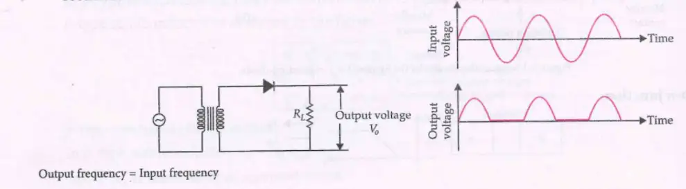
Half Wave Rectifier
- Diode conducts during positive half cycle only.
- Output is unidirectional pulsating DC.
- Output frequency = input frequency.
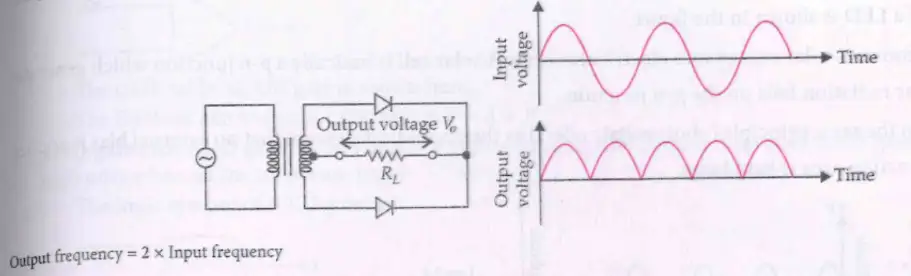
Full Wave Rectifier
- Rectifies both positive and negative half cycles.
- Uses two diodes and transformer with center tap.
- Output frequency = 2 × input frequency.
- Output is smoother pulsating DC.
Solved Examples
Ex 1
Calculate output frequency of full wave rectifier if input AC frequency is 50 Hz.
- Output frequency = 2 × 50 Hz = 100 Hz.
Practice Set
Q1: What is the output frequency of a half wave rectifier if input frequency is 60 Hz?
- A) 30 Hz
- B) 60 Hz
- C) 120 Hz
- D) 0 Hz
Q2: In a full wave rectifier, the output frequency is:
- A) Same as input frequency
- B) Twice the input frequency
- C) Half the input frequency
- D) Zero
Q3: Which component is essential for full wave rectification?
- A) One diode
- B) Two diodes and center-tapped transformer
- C) Capacitor only
- D) Resistor only
Answer Key
Q1: B) 60 Hz - Half wave rectifier output frequency equals input frequency.
Q2: B) Twice the input frequency - Full wave rectifier doubles frequency.
Q3: B) Two diodes and center-tapped transformer - Required for full wave rectification.
Memory Aids
- Half wave: Output frequency = input frequency.
- Full wave: Output frequency = 2 × input frequency.
- Full wave needs two diodes + center tap.
Special Purpose p-n Junction Diodes
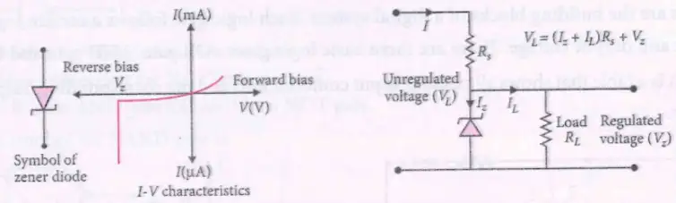
Zener Diode
- Heavily doped p-n junction diode.
- Operates in reverse bias.
- Zener voltage \(V_Z\) remains constant over wide current range.
- Used as voltage regulator.
- Voltage across Zener diode remains constant despite input voltage changes.
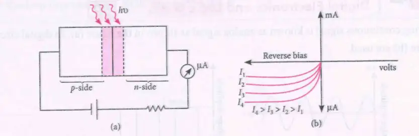
Photodiode
- Special p-n junction diode with transparent window.
- Operated under reverse bias.
- Generates photocurrent proportional to light intensity.
- Used in light sensors and cameras.
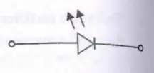
Light Emitting Diode (LED)
- Converts electrical energy into light energy.
- Heavily doped p-n junction diode.
- Emits light under forward bias.
- Threshold voltage higher than Si diode; varies with color.
- Reverse breakdown voltage ~5 V.
- Made from GaAsP (visible colors) or GaAs (infrared).
Solar Cell
- Converts solar energy into electrical energy.
- Large area p-n junction generating emf on illumination.
- Works on photovoltaic effect (no external bias).
Solved Examples
Ex 1
What happens to Zener diode voltage when input voltage increases?
- Voltage across Zener diode remains constant.
Practice Set
Q1: Zener diode is used as a:
- A) Rectifier
- B) Voltage regulator
- C) Light emitter
- D) Photodetector
Q2: Photodiode operates under:
- A) Forward bias
- B) Reverse bias
- C) No bias
- D) Both biases
Q3: LED emits light when:
- A) Reverse biased
- B) Forward biased
- C) No bias
- D) Under illumination
Answer Key
Q1: B) Voltage regulator - Zener diode maintains constant voltage.
Q2: B) Reverse bias - Photodiode works in reverse bias.
Q3: B) Forward biased - LED emits light under forward bias.
Memory Aids
- Zener diode: Reverse bias, constant voltage \(V_Z\).
- Photodiode: Reverse bias, current ∝ light intensity.
- LED: Forward bias, electrical to light energy.
- Solar cell: Photovoltaic effect, no external bias.
Digital Electronics and Logic Gates
Signals
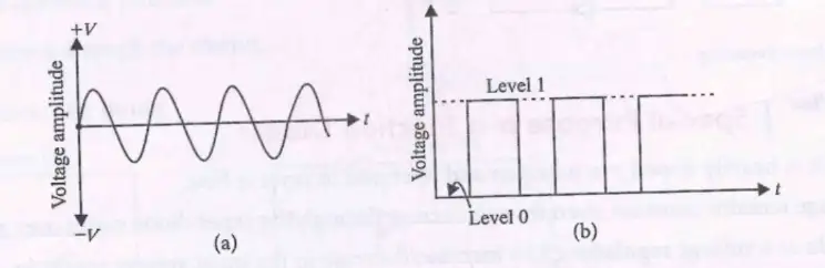
- Analog signal: Continuous time-varying voltage.
- Digital signal: Two discrete levels (0 and 1).
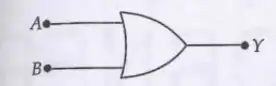
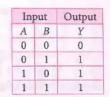
OR Gate
- Two or more inputs, one output.
- Output is high if any input is high.
- Boolean expression: \(Y = A + B\).
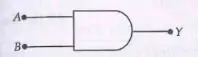
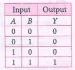
AND Gate
- Two or more inputs, one output.
- Output is high only if all inputs are high.
- Boolean expression: \(Y = A \cdot B\).
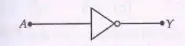
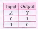
NOT Gate
- One input, one output.
- Output is inversion of input.
- Boolean expression: \(Y = \overline{A}\).
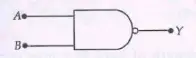
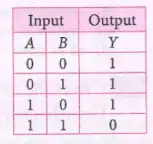
NAND Gate
- AND gate followed by NOT gate.
- Output is low only if all inputs are high.
- Boolean expression: \(Y = \overline{A \cdot B}\).
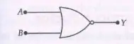
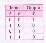
NOR Gate
- OR gate followed by NOT gate.
- Output is high only if all inputs are low.
- Boolean expression: \(Y = \overline{A + B}\).
Solved Examples
Ex 1
Find output of OR gate when inputs A=0, B=1.
- Output \(Y = 0 + 1 = 1\).
Practice Set
Q1: Output of AND gate when A=1, B=0 is:
- A) 0
- B) 1
- C) Undefined
- D) 2
Q2: Boolean expression for NAND gate is:
- A) \(Y = A + B\)
- B) \(Y = \overline{A \cdot B}\)
- C) \(Y = A \cdot B\)
- D) \(Y = \overline{A + B}\)
Q3: Output of NOT gate when input is 0 is:
- A) 0
- B) 1
- C) Undefined
- D) 2
Answer Key
Q1: A) 0 - AND gate output is 1 only if both inputs are 1.
Q2: B) \(Y = \overline{A \cdot B}\) - NAND is NOT of AND.
Q3: B) 1 - NOT gate inverts input.
Memory Aids
- OR: Output high if any input high.
- AND: Output high only if all inputs high.
- NOT: Output is inverse of input.
- NAND: AND followed by NOT.
- NOR: OR followed by NOT.
NEET Physics — ALL CHAPTERS
1
Basic Mathematics
2
Units and Measurement
3
Motion in a Straight Line
4
Motion in a Plane
5
Laws of Motion
6
Work, Energy and Power
7
System of Particles and Rotational Motion
8
Gravitation
9
Mechanical Properties of Solids
10
Mechanical Properties of Fluids
11
Thermal Properties of Matter
12
Thermodynamics
13
Kinetic Theory
14
Oscillations
15
Waves
16
Electric Charges and Fields
17
Electrostatic Potential and Capacitance
18
Current Electricity
19
Moving Charges and Magnetism
20
Magnetism and Matter
21
Electromagnetic Induction
22
Alternating Current
23
Electromagnetic Waves
24
Ray Optics and Optical Instruments
25
Wave Optics
26
Dual Nature of Radiation and Matter
27
Atoms
28
Nuclei
29
Semiconductor Electronics: Materials, Devices and Simple Circuits